When designs become smaller, faster, and more complex, ensuring stable signal transmission and power delivery becomes increasingly challenging.
As an electronics engineer, understanding and addressing signal & power integrity issues is critical to your design’s performance. It can mean the difference between a successful product and failures during production or in the field.
Signal transmission is affected by noise, crosstalk, or electromagnetic interference (EMI).
Power delivery to components is unstable or inefficient, leading to operational issues.
Reflections and signal delays cause problems in high-frequency circuits.
Minimizing losses and ensuring proper impedance matching in the design is difficult.
Supply voltage fluctuates unacceptably due to voltage drops or transients.
The design requires multiple iterations to resolve signal or power-related issues, delaying projects and increasing costs.
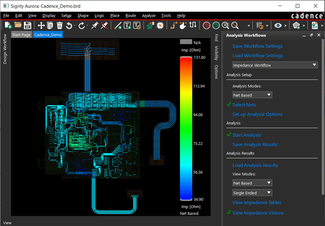
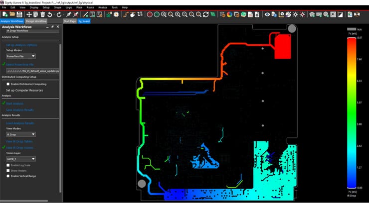
With Cadence® Sigrity™ PowerDC™, you get added accuracy of electrical/thermal co-simulation, as well as the assurance that your PDN performs as expected. With PowerDC, you can easily locate accidental voltage losses, high current densities, via with excessive currents and thermal hotspots. All these effects can significantly affect the quality of the design and limit the life of the product.

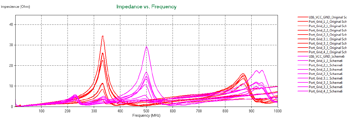
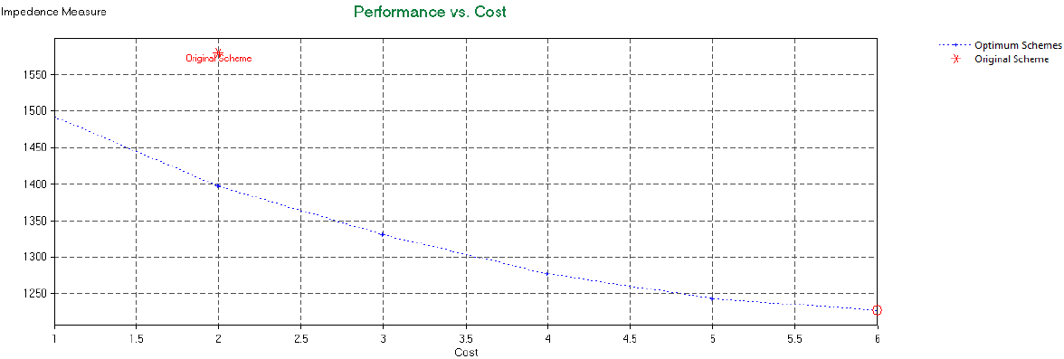
With Cadence® Sigrity™ OptimizePI™, you get insight into how the PDN frequency characteristics look for each individual component, including the planes shape and placement in the stackup, decoupling their routing and placement, as well as routing from supply plans to components. Decouplings can also be optimised in terms of price vs. performance and verify EMI performance by measuring impedance for self-selected locations on the layout.

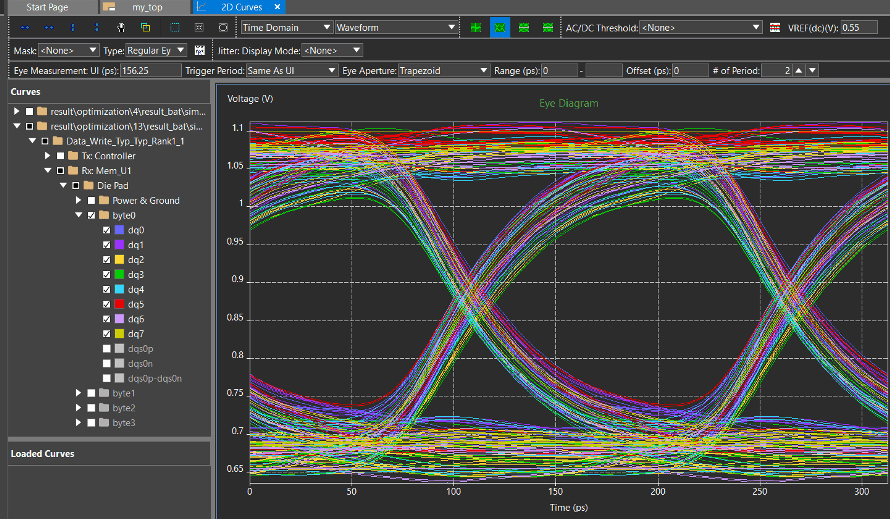
Perform chip-to-chip analysis on highspeed SerDes interfaces, such as PCI Express® (PCIe®), HDMI, SFP+, Xaui, Infiniband, SAS, SATA, and USB with industry-standard IBIS AMI models.
You can run pre-layout analyses using templates, and add models of component packages, connectors, and layouts to reflect the entire interface.
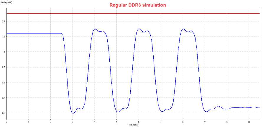
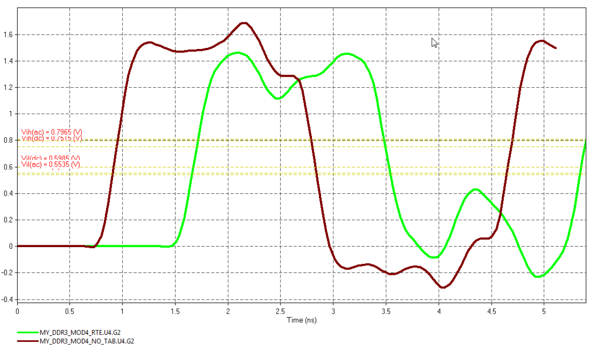
Run simulations to identify crosstalk problems and show the signals in the interface, as well as signals after clock and data recovery (CDR), which are described in the IBIS AMI model.
By simulating the complete interface with millions of bits, the overall bit error rate (BER) can be calculated to determine whether jitter and noise levels are within specified tolerances.